さらに必要ですか?
| 数量 | 価格(税込み) |
|---|---|
| 1+ | ¥111.02 (¥122.122) |
| 10+ | ¥70.96 (¥78.056) |
| 100+ | ¥57.77 (¥63.547) |
| 500+ | ¥55.19 (¥60.709) |
| 1000+ | ¥53.1 (¥58.41) |
| 2500+ | ¥50.85 (¥55.935) |
| 5000+ | ¥49.4 (¥54.34) |
製品情報
製品概要
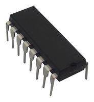
The CD4042BE is a CMOS Quad-clocked 'D' Latch, each strobed by a common clock. Complementary buffered outputs are available from each circuit. The impedance of the n and p-channel output devices is balanced and all outputs are electrically identical. Information present at the data input is transferred to outputs Q and Q\ during the CLOCK level which is programmed by the POLARITY input. For POLARITY=0 the transfer occurs during the 0 CLOCK level and for POLARITY=1 the transfer occurs during the 1 CLOCK level. The outputs follow the data input providing the CLOCK and POLARITY levels defined above are present. When a CLOCK transition occurs (positive for POLARITY=0 and negative for POLARITY=1) the information present at the input during the CLOCK transition is retained at the output until an opposite CLOCK transition occurs.
- Clock polarity control
- Q and Q\ outputs
- Common clock
- Low power TTL compatible
- Standardized, symmetrical output characteristics
- 100% Tested for quiescent current at 20V
技術仕様
CD4042
差動
6.8mA
DIP
3V
4ビット
4042
125°C
CD4000 LOGIC
0
D タイプ
40ns
DIP
16ピン
18V
CD4000
-55°C
-
0
技術文書 (1)
法律および環境情報
最後に重要な製造工程が行われた国生産国:Malaysia
最後に重要な製造工程が行われた国
RoHS
RoHS
製品コンプライアンス証明書
