Key design strategies for effective ESD mitigation in electronics
Electrostatic Discharge (ESD) is a pervasive issue in the field of electronics, posing a substantial threat to the integrity and longevity of electronic circuits.
Electrostatic Discharge (ESD) presents a significant risk to electronic circuits as it can cause immediate or long-term damage to sensitive components. ESD occurs when a brief electric current surges between two electrically charged objects triggered by contact, dielectric breakdown, or an electrical short. It is essential to classify ESD into device-level and system-level occurrences to understand its impact on electronic parts. Device-level ESD occurs in a semiconductor assembly within a controlled ESD environment, while system-level ESD affects a fully assembled electronic product. Device-level ESD is particularly harmful and requires protection for electronic components, whether mounted on a printed circuit board (PCB) or not.
ESD failures can range from subtle to catastrophic. Soft failures are temporary changes in internal logic or data stream corruption. Latent defects happen when ESD damages components, leading to gradual functionality degradation and premature failure. Catastrophic failures are characterized by complete damage to the element due to ESD.
ESD fundamentals
In industrial environments, static charge generation and transfer mainly happen through two processes:
- Triboelectric charging
- Electrostatic induction
Triboelectric charging:
This occurs when two materials of different types touch and then part ways, and electrons swap between their surfaces. This exchange leaves one material positively charged and the other negatively charged. The extent of charge separation is influenced by the specific materials involved and their relative positions on the triboelectric series, which ranks materials based on their electron-donating or accepting tendencies. In industrial settings, triboelectric charging often occurs during various processes involving the movement or contact of materials, such as:
Material handling:
Friction between objects during handling, transportation, or packaging can cause triboelectric charging.
Machinery operation:
Moving parts and machinery components can generate static charges through frictional contact.
Manufacturing processes:
Operations involving plastics, textiles, and rubbers are prone to triboelectric charging due to their insulating properties.
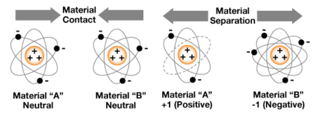
Figure 1: Triboelectric charging (Source)
The accumulation of static charges on surfaces increases the risk of ESD when charged objects make contact with sensitive electronic components. Learn more about Triboelectric charging here.
Electrostatic induction:
This occurs when a charged object induces an opposite charge on a nearby object without direct contact. This process relies on the electrostatic forces between charged particles.
In industrial settings, electrostatic induction can occur in various scenarios, including:
Proximity to charged objects: Sensitive electronic components may become charged through proximity to other charged objects, such as machinery or equipment with static buildup.
Nearby electrical fields: External electrical fields from power sources or machinery can induce charges on nearby conductive or semiconductive surfaces.
Process-related factors: Temperature, humidity, or pressure changes can influence electrostatic induction processes within industrial environments.
Electrostatic induction poses an ESD risk when induced charges accumulate on surfaces and discharge upon contact with grounded or oppositely charged objects, potentially damaging sensitive electronics.
Device-level ESD control strategies
Device-level ESD control strategies are crucial due to the high susceptibility of electronic components to ESD damage. Understanding ESD susceptibility helps in implementing effective measures to protect these sensitive components. Electronic components and Integrated circuits (ICs) are highly susceptible to ESD due to their sensitive semiconductor materials, compact size, and limited surface area for dissipating excess energy. Generally, smaller geometries and thinner dielectric layers make components more susceptible to ESD. The high voltages and currents from ESD events can lead to dielectric breakdown, junction damage, or physical harm to the component's structure. Components are classified by their ESD sensitivity, ranging from highly sensitive to robust.
ESD susceptibility testing models commonly used in the industry:
ESD susceptibility is evaluated using standardized tests like the Human Body Model (HBM), Charged Device Model (CDM), Floating Device Model (FICM), and Machine Model (MM). These tests simulate different ESD scenarios and measure the component's resilience.
HBM- The Human Body Model (HBM) is the most widely used model for determining the susceptibility of an electronic device to ESD damage. It replicates a situation where a charged person or object comes into contact with a device with one or multiple connections directly or resistively to the ground. A mere touch or proximity of a finger to the leads of an ESDS item can cause discharge, potentially damaging the device. The HBM aims to describe how an ESD event from the human body could discharge current into a protected circuit.
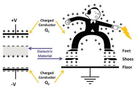
Figure 2: Human Body Model (HBD) (Source)
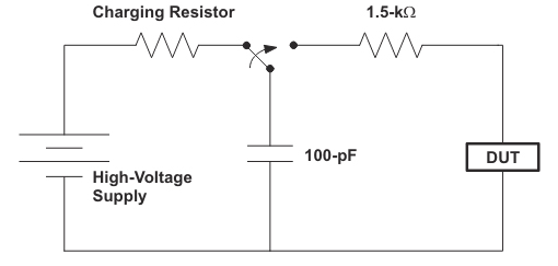
Figure 3: Equivalent circuit of Human Body Model (Source)
CDM- Charged Device Model (CDM) testing standards establish the ESD susceptibilities of integrated circuits (ICs). CDM simulates scenarios in electronics manufacturing or handling where a static-sensitive device charges and discharges to a conductor. This testing recreates potentially destructive discharge mechanisms in automated component handling systems and similar situations during semiconductor packaging and assembly. The accumulation of high charges in components rapidly discharges upon encountering a lower electrostatic level conductor, often resulting in dielectric breakdown and failure. With peak currents reaching tens of amperes within nanoseconds, this low-impedance, metal-to-metal charge transfer poses significant risks.
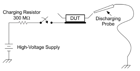
Figure 4: CDM Discharge and the Device Equivalent Circuit (Source)
FDI - The Floating Device Model (FDM) simulates scenarios where a charged person or object touches a device while its pins remain ungrounded. Like CDM, this model's damage mechanism stems from large voltage gradients coupling into various chip areas. Unlike the CDM, damage occurs during device charging rather than discharge. Like the CDM, the device's capacitance to ground is crucial in determining susceptibility.
MM- The Machine Model (MM) is used in scenarios where machines rather than humans handle components and PCBs. When a machine discharges through component connections, it offers a low-resistance, rapid discharge path. The machine's capacitance is significantly higher than a human's, leading to a higher stored charge quantity. Damage from an MM discharge typically manifests with lower potential compared to an HBM discharge. The MM model simulates a direct discharge from charged assembly equipment, fixtures, or tools through a component to the ground.
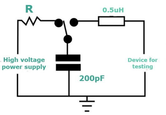
Figure 5: Equivalent machine model circuit
System-level ESD control strategies
System-level ESD protection strategies depend on physical design, operational requirements, and cost. Various protection methods are used to minimize ESD coupling. A robust ESD design considers multiple elements such as:
ESD-safe materials:
ESD-safe materials mitigate static electricity discharge, safeguarding products from damage. These are extensively used in areas where static-sensitive electronic components and devices are handled or manufactured. ESD-safe materials are categorized based on surface resistivity into three types:
- Conductive materials: These have a surface resistivity of less than 1 x 10E5 Ω/square or volume resistivity of less than 1 x 10E4 Ωcm. Conductors enable fast electron flow across surfaces or through volumes.
- Static dissipative materials: Their surface resistivity is greater or equal to 1 x 10E5 Ω/square but greater than 1 x 10E12 Ω/square, or volume resistivity between 1 x 10E4 Ωcm and 1 x 10E11 Ωcm. Charge flows slower in static dissipative materials, leading to lower-energy arcs during discharge, ideal for protecting devices from ESD damage.
- Insulative materials: These have a surface or volume resistance equal to or greater than 1 x 10E11 Ω. Insulators like plastics have high electrical resistance, preventing the flow of charge. Adding conductive particles can alter their conductivity.
- The critical applications of these materials include:
- Electronics manufacturing environments for custom jigs, tools, and fixtures, enabling high-volume production.
- Laboratory setups, housing, and specialized equipment for handling sensitive electronics.
- Versatile use across various applications, enabling safe handling, maintaining quality, and cost-effectiveness.
| Antistatic type | Static-Dissipative type | Conductive type | |
|---|---|---|---|
| Surface Resistivity (Ohm/Cm) | 1010 - 1012 | 106 - 1010 | 102 - 106 |
| Charge | Initial electrostatic charges suppressed | Little or no initial charge, prevent discharge from human contact | No initial charge, creates pathway for energy to disperse |
| Treatment | Filled with carbon powder, carbon fiber or coated carbon fiber | Filled with carbon powder, carbon fiber or coated carbon fiber | Filled with carbon powder, carbon fiber or stainless steel |
| Materials | ABS Acetal Polycarbonate | ABS Acetal Polycarbonate | ABS Acetal Polycarbonate |
| Polypropylene PDVF UHMW-PE | Polypropylene PDVF UHMW-PE | Polypropylene PDVF UHMW-PE |
ESD Product testing:
ESD testing assesses a device's vulnerability to electrostatic discharge, ensuring compliance with ESD protection standards. The typical testing equipment is:
- Wrist strap tester: This device, available in portable or wall-mounted options, tests the grounding effectiveness of the user's wrist strap with a plug-in system, displaying results through a color-coded system (green for pass, red for failure).
- Footwear testing: Regular testing of ESD footwear is often integrated with wrist strap testing stations, ensuring compliance within the range of 750 Kilohms to 100 Megohms for safe EPA.
- Electrical surface resistivity tester: Handheld meters or kit components are commonly used to measure point-to-point ESD resistance and surface resistivity, providing high accuracy within a static dissipative range of 10 to 100 volts.
- Constant Monitors: They continuously check wrist straps, bench mats, and Earth connections for disconnection, ensuring uninterrupted ESD protection.
- Electrostatic field monitors: Compact, handheld ESD meters and kits enable precise measurement of static charges in workplaces, particularly suited for low light and confined areas, ensuring accurate monitoring for EPA environments.
ESD flooring:
ESD flooring prevents static electricity buildup and safeguards against static electricity accumulation. Effective static-control floors have two vital tasks: creating a traceable ground path and reducing static generation, ensuring people remain unchanged as they move. The most effective ESD flooring techniques involve conductive floor coatings and ESD tiles. Conductive floor coating includes the following steps-
- Subfloor or substrate: Use a multi-layer structure with a subfloor composed of cement-bound substrates like concrete screeds or magnesia/anhydrite screeds.
- Primer coating: Apply a solvent-free, low-viscosity epoxy resin primer, which can be filled with quartz sand to create a leveling layer.
- Filling and Leveling coat: Level uneven subfloors with a filler coat composed of resin primers and quartz sands, ensuring a smooth and level base for the subsequent layers.
- Conductive Layer/Grounding: Apply a conductive layer to channel static discharge to the ground. Grounding is established using self-adhesive tinned copper strips or conducting sets.
- Finishing Coat: Incorporate either carbon fibers or special conductive fillers to impart conductivity to the system. Various options are available for different requirements.
- Sealing: Apply pigmented conductive sealings that meet ESD standards and are also high abrasion resistant.
- ESD floor tiles contain conductive elements like carbon or graphite for electrical conductivity. They're installed on the top of an electrically conductive underlayment, which serves as a unified ground plane. Copper grounding strips connect to an electrical outlet or earth ground, allowing static electricity to dissipate safely.
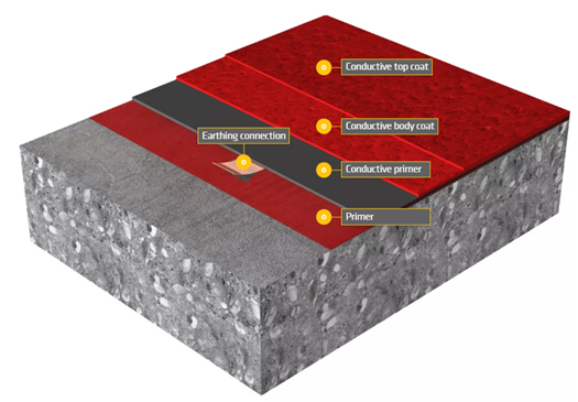
Figure 6: ESD tiles working principle (Source)
ESD standards
ESD standards are essential for managing electrostatic discharge (ESD) and establishing protected environments. These standards define product sensitivity to ESD and prescribe specific measures for environments prone to electrostatic fields. Accredited by ANSI, the EOS/ESD Association develops ESD standards and testing methods. A few notable ESD standards are:
- ANSI/ESD S20.20-2021: Protection of electrical and electronic parts.
- International Electrotechnical Commission IEC 61340-5-1: General requirements for protecting electronic devices from electrostatic phenomena.
- ANSI/ESD S8.1-2021: Standard symbols for protecting electrostatic discharge susceptible items.
- ANSI/ESD S6.1-2019: Guidelines for electrostatic discharge grounding.
- ANSI/ESD S541-2019: Standard packaging for ESD susceptible materials.
Conclusion
Effective strategies to mitigate electrostatic discharge (ESD) are crucial to protecting electronic circuits from damage. The guide proceeds to discuss device-level ESD control strategies, emphasizing the importance of testing models such as the Human Body Model (HBM), Charged Device Model (CDM), Floating Device Model (FDM), and Machine Model (MM). These models help simulate real-world ESD scenarios, providing valuable insights into a component's resilience. This guide aims to equip engineers and technicians with the knowledge and tools necessary to design robust and reliable electronic devices that can withstand the challenges posed by ESD.


